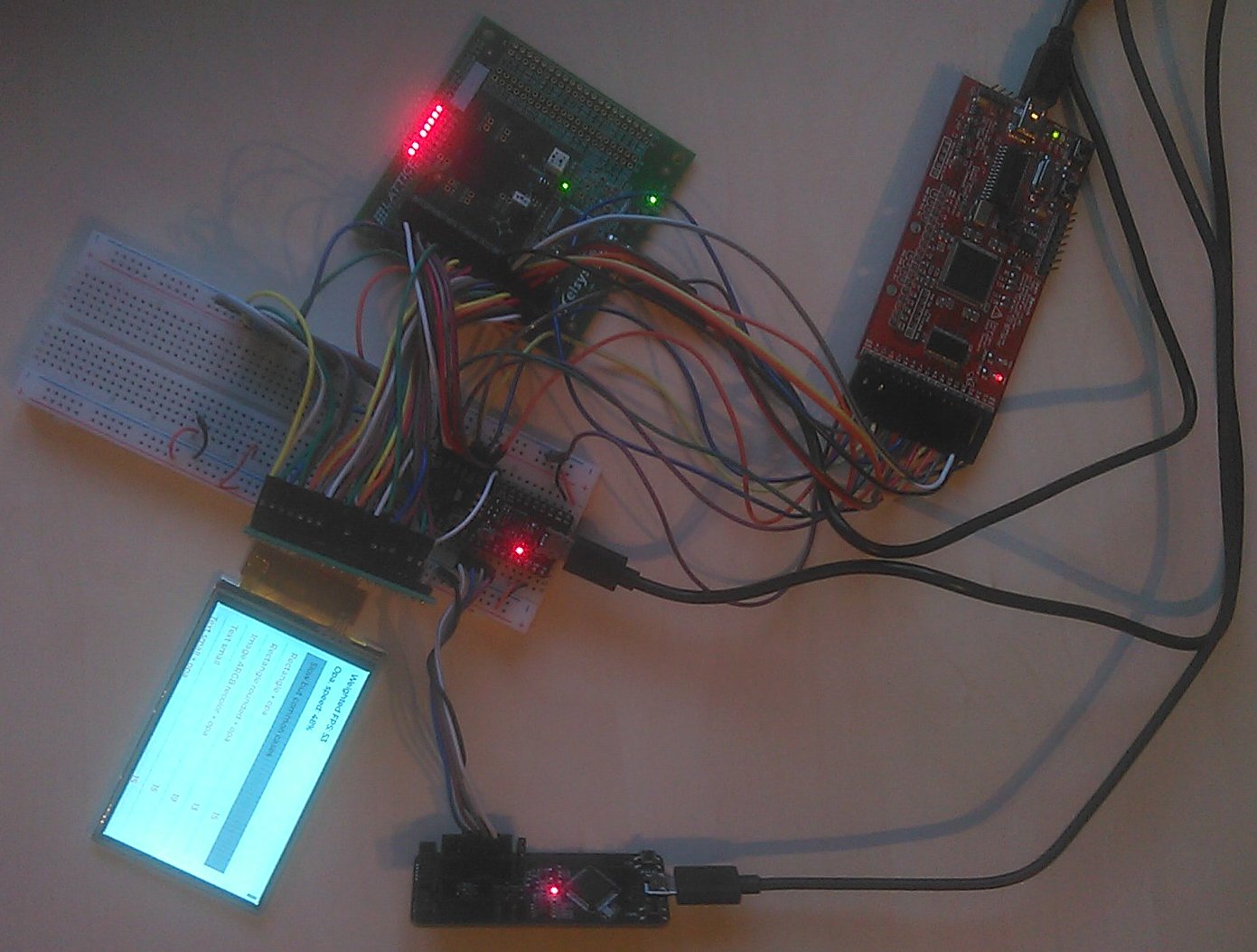
I done proof-of-concept to use QSPI to feed display data in parallel with small FPGA converter.
I tested support of ILI9481 with IPS display (~ $7, 3.5" 480x320px) with standard SPI access “ESP32 -> { MOSI, SCLK, CS, D/C, RESET } -> ILI9481 (DBI Type C 8-bit)” but it works only to 16 MHz (~2MB/s) and benchmark is 6FPS.
So, I took some FPGA and did some converter “ESP32 -> { SCLK, CS, 4x DATA } -> FPGA -> { 16x DATA, CS, D/C, RESET } -> ILI9481 (DBI Type B 16-bit)”. QSPI is running @ 40 MHz (~20MB/s) and parallel interface is running @ 10 MHz (compliant with datasheet without overclocking). Much better now - benchmark is 53FPS !
Benchmark (CONFIG_ESP32_DEFAULT_CPU_FREQ_MHZ=240, CONFIG_COMPILER_OPTIMIZATION_PERF=y, CONFIG_FREERTOS_HZ=1000):
As far as I understand it, you’re using the FPGA only as a converter from QSPI to 16bit 8080 interface, right? Wouldn’t it be possible to achieve the same with serial-in-parallel-out shift registers, instead of an FPGA?
Not exactly. For QSPI (4bit) at least 3x 4bit D-latch, shift register to select clk to latch, glue logic to cycle shift register and generate WRCLK, from ESP32 need more software signaling (CS,DC and new data8 vs. data16 latching (for color xfer)) … try to build it .
There are also some challenges:
setup/hold times for data versus clock and additional glue logic
you must change QSPI speed (16bit color data vs. 8bit paramaters xfers) to respect datasheet
PCB place
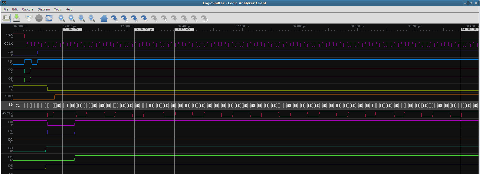
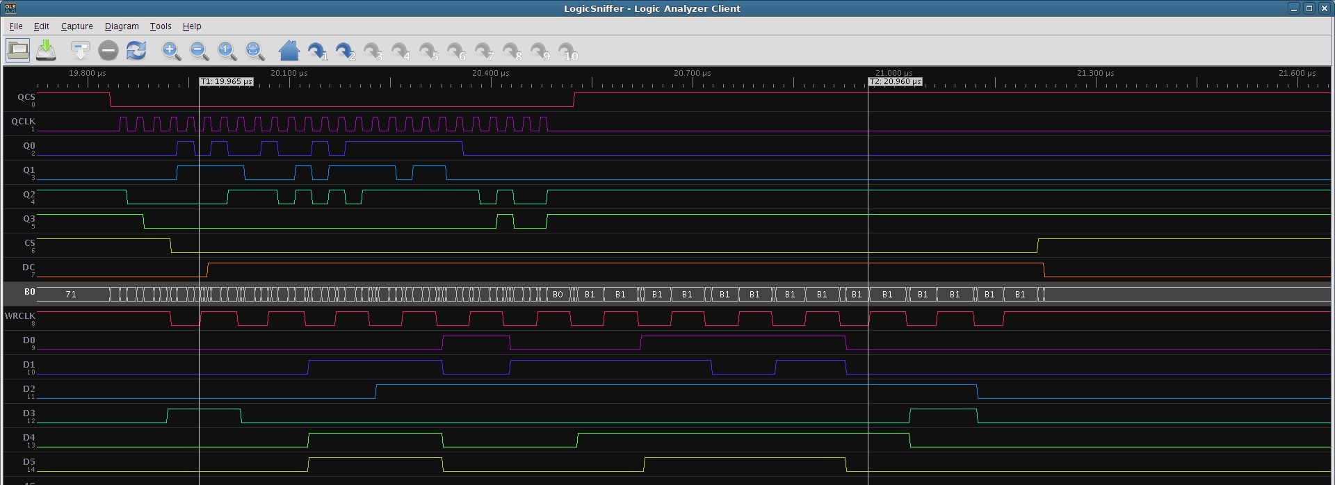
I added programmable maximum WRCLK rate (specific SPI command) with FIFO buffer, also programmable data xfer command automatic detection (ILI9481_CMD_MEMORY_WRITE, ILI9481_CMD_WRITE_MEMORY_CONTINUE) and prepared for HW color conversions (byte swapping, RGB888->RB565, XRGB8888>RB565, …)…
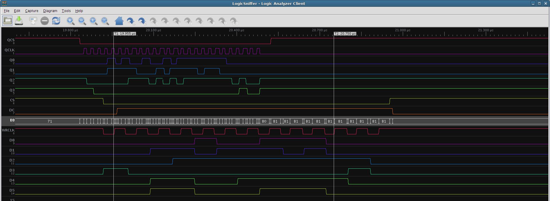
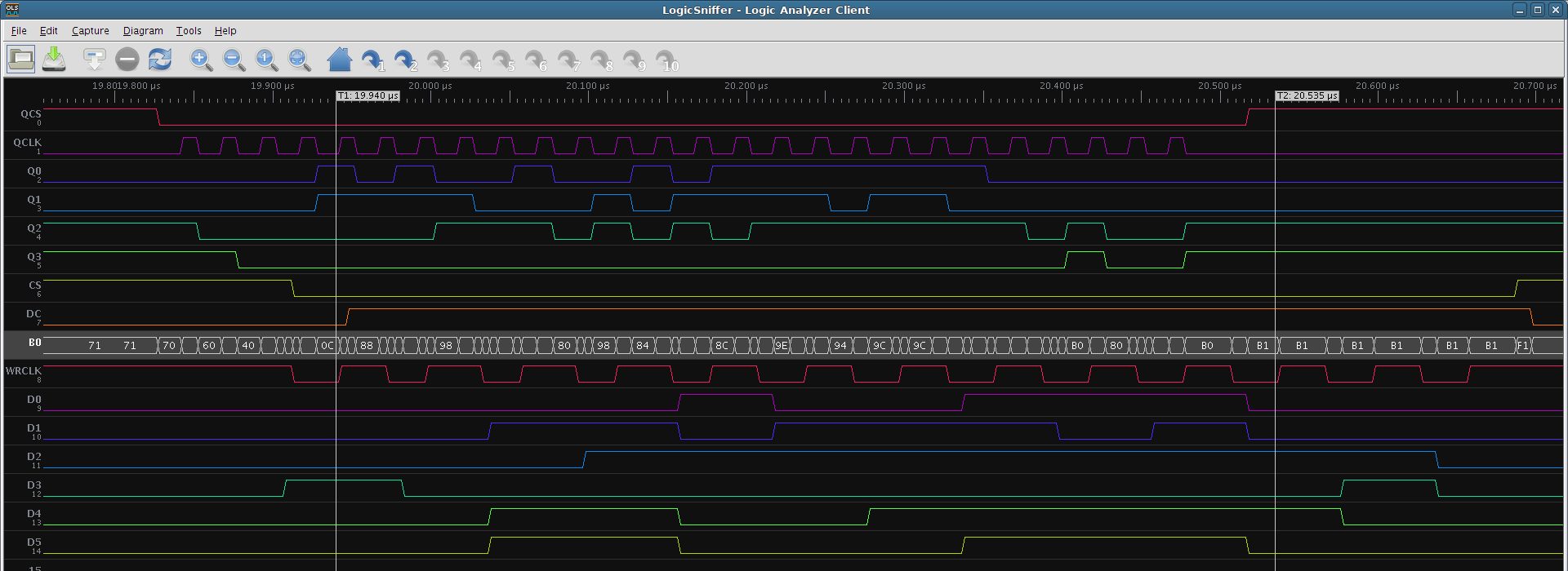
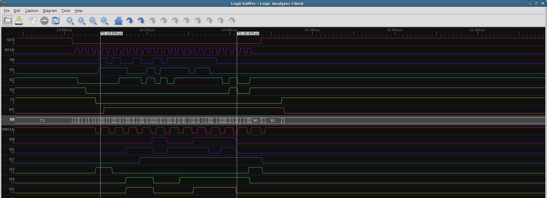
Example for FPGA (ILI9481_CMD_GAMMA_SETTING) - by datasheet “twc - Write cycle - 100ns” => 10MHz:
The simplest solution can be achieved with 8-bit only xfers (DBI Type B 8-bit) I think that it will be 5x D-flop needed. But limited QSPI to 20MHz only (10MB/s). I will try sometimes.
It is FPGA not memory chip. FPGA is programmable chip do everything you want and very fast. I use this as QSPI → 8080parallel smart bridge for LCD panel in this case. FPGA usually have some small embedded memories (I use this for FIFO queue between different clock domains).
If you query for QSPI PSRAM - there are few manufacturers. ESP32 supported.
@mcerveny I’m interested in trying your approach as well, but with a different hardware (Xilinx FPGA that already does other stuff, and SSD1963 graphics chip). Some more questions:
Do I understand correctly that you have come up with an SPI protocol which has commands to manipulate the extra pins?
If so, I assume you have something like a state machine within the FPGA and you reset it to a starting state when the incoming CS goes low, then you treat the first byte (or first nibble?) as an opcode, and the rest as data until CS goes high again? So you presumably have four opcodes to set D/C and RESET high and low, and another two opcodes for sending 8bit and 16bit data - and those would handle the outgoing CS, concatenate the nibbles to 8 respectively 16 bits and then clock the outgoing SCK once the desired width is full? And that is where you have the FIFO, so the output speed can be independent of the input speed as long as the FIFO doesn’t get full?
I haven’t done much with ESP32… are you sharing the same QSPI pins where also the flash of the module is connected? And if so, does it work without interfering just by having a seperate CS, or do you need to take precautions so that transactions don’t overlap?
It would be great to hear more about your protocol and maybe see some code and HDL!
…thinking this a bit further, there is not much missing for turning this into a graphics controller of its own which can drive a (much cheaper) controller-less display directly! The tricky thing about driving a controller-less display is the timing. You have solved this already. You’d need a bigger FIFO, but probably it wouldn’t be necessary to have a frame buffer in (or attached to) the FPGA, since LVGL outputs the pixels from top-left to bottom-right anyways. The circuit would have to buffer a few lines maybe and genereate the HSYNC and VSYNC signals. That should fit in very low-end FPGAs which don’t have much memory. Pretty exciting!
cfg_wait - cfg_wait_lo+cfg_wait_hi - programmable minimum high and low WRCLK output
cfg_data_cmd1 and cfg_data_cmd2 - programmable command for data feed (switching CMD output)
All input data from QSPI are copied to output (4->8 bit conversion, except config 0xff) (see DBI Type B protocol) over FIFO (~16 depth) with automatic recognition of data command (that makes data accumulation & conversion).
No. ESP32 have three SPI/QSPI interfaces. I use VSPI.
There is my Veriliog code (see previous post screenshot from ICE studio):
// Copyright 2020, Martin Cerveny
// SPDX-License-Identifier: CERN-OHL-P-2.0+

module convertor (
 input clk,
 input spi_clk,
 input spi_cs,
 input [3:0] spi_d,
 output rst,
 output cs,
 output wrclk,
 output cmd,
 output latch1,
 output latch2,
 output [7:0] data,
 output [15:0] debug
);

// SPI clock domain

localparam
    FSM_SPI_CMD = 0,

    FSM_SPI_CFG1 = 1,
    FSM_SPI_CFG2 = 2,
    FSM_SPI_CFG3 = 3,
    FSM_SPI_CFG4 = 4,

    FSM_SPI_PARAM = 5,

    FSM_SPI_1DATA0 = 6,

    FSM_SPI_2DATA0 = 7,
    FSM_SPI_2DATA1 = 8,

    FSM_SPI_3DATA0 = 9,
    FSM_SPI_3DATA1 = 10,
    FSM_SPI_3DATA2 = 11,

    FSM_SPI_4DATA0 = 12,
    FSM_SPI_4DATA1 = 13,
    FSM_SPI_4DATA2 = 14,
    FSM_SPI_4DATA3 = 15;

localparam
    CMD_CFG = 8'hff;

localparam
    WHAT_BYTE = 0,
    WHAT_CONVERT = 1;

// SPI
reg [3:0] upper;
reg [3:0] fsm_spi = FSM_SPI_CMD, fsmnext_spi;
reg fsm_upper;
reg [2:0] spi_cs_debouncer;

// SPI to QUEUE
reg [31:0] spi_data;
reg [0:0] spi_what;
reg [2:0] spi_data_req_cdc;
reg spi_data_req;

// configuration
reg [7:0] cfg, cfg_wait, cfg_data_cmd1, cfg_data_cmd2;

assign rst = cfg[7];
wire [1:0] spi_data_size = cfg[6:5];
wire [4:0] convert = cfg[4:0];
wire [3:0] cfg_wait_lo = cfg_wait[3:0];
wire [3:0] cfg_wait_hi = cfg_wait[7:4];

wire [7:0] spi_byte = { upper, spi_d };
wire spi_cs_debounced = spi_cs & spi_cs_debouncer[2] & spi_cs_debouncer[1];

assign debug = { data, wrclk, cmd, cs };

// FSM TRANSITION WITH QSPI HI-LO

always @(posedge spi_clk or posedge spi_cs_debounced)
begin
    if (spi_cs_debounced)
        begin
            fsm_upper <= 0;
            fsm_spi <= FSM_SPI_CMD;
        end
    else
        if (fsm_upper)
            begin
                fsm_upper <= 0;
                fsm_spi <= fsmnext_spi;
            end
        else
            begin
                upper <= spi_d;
                fsm_upper <= 1;
            end
end

// FSM NEXT STATE

always @* begin
    fsmnext_spi = fsm_spi;
    case (fsm_spi)
        FSM_SPI_CMD:
            begin
                if (spi_byte == CMD_CFG) fsmnext_spi = FSM_SPI_CFG1;
                else if (spi_byte == cfg_data_cmd1 || spi_byte == cfg_data_cmd2)
                    case (spi_data_size)
                        0: fsmnext_spi = FSM_SPI_1DATA0;
                        1: fsmnext_spi = FSM_SPI_2DATA0;
                        2: fsmnext_spi = FSM_SPI_3DATA0;
                        3: fsmnext_spi = FSM_SPI_4DATA0;
                    endcase
                else fsmnext_spi = FSM_SPI_PARAM;
            end

        FSM_SPI_CFG1: fsmnext_spi = FSM_SPI_CFG2;
        FSM_SPI_CFG2: fsmnext_spi = FSM_SPI_CFG3;
        FSM_SPI_CFG3: fsmnext_spi = FSM_SPI_CFG4;

        FSM_SPI_2DATA0: fsmnext_spi = FSM_SPI_2DATA1;
        FSM_SPI_2DATA1: fsmnext_spi = FSM_SPI_2DATA0;

        FSM_SPI_3DATA0: fsmnext_spi = FSM_SPI_3DATA1;
        FSM_SPI_3DATA1: fsmnext_spi = FSM_SPI_3DATA2;
        FSM_SPI_3DATA2: fsmnext_spi = FSM_SPI_3DATA0;

        FSM_SPI_4DATA0: fsmnext_spi = FSM_SPI_4DATA1;
        FSM_SPI_4DATA1: fsmnext_spi = FSM_SPI_4DATA2;
        FSM_SPI_4DATA2: fsmnext_spi = FSM_SPI_4DATA3;
        FSM_SPI_4DATA3: fsmnext_spi = FSM_SPI_4DATA0;

    endcase
end

// FSM EXEC

always @(posedge spi_clk or posedge spi_cs_debounced)
begin
    if (spi_cs_debounced)
        begin
            spi_data_req <= 0;
        end
    else
        if (fsm_upper)
            case (fsm_spi)
                FSM_SPI_CMD:
                    if (fsmnext_spi != FSM_SPI_CFG1)
                        begin
                            spi_data[7:0] <= spi_byte;
                            spi_what <= WHAT_BYTE;
                            spi_data_req <= 1;
                        end

                FSM_SPI_CFG1:
                    cfg <= spi_byte;
                FSM_SPI_CFG2:
                    cfg_wait <= spi_byte;
                FSM_SPI_CFG3:
                    cfg_data_cmd1 <= spi_byte;
                FSM_SPI_CFG4:
                    cfg_data_cmd2 <= spi_byte;

                FSM_SPI_PARAM:
                    begin
                        spi_data[7:0] <= spi_byte;
                        spi_what <= WHAT_BYTE;
                        spi_data_req <= 1;
                    end

                FSM_SPI_1DATA0:
                    begin
                        spi_data[7:0] <= spi_byte;
                        spi_what <= WHAT_CONVERT;
                        spi_data_req <= 1;
                    end

                FSM_SPI_2DATA0,
                FSM_SPI_3DATA0,
                FSM_SPI_4DATA0: spi_data[7:0] <= spi_byte;

                FSM_SPI_2DATA1:
                    begin
                        spi_data[15:8] <= spi_byte;
                        spi_what <= WHAT_CONVERT;
                        spi_data_req <= 1;
                    end

                FSM_SPI_3DATA1,
                FSM_SPI_4DATA1: spi_data[15:8] <= spi_byte;

                FSM_SPI_3DATA2:
                    begin
                        spi_data[23:16] <= spi_byte;
                        spi_what <= WHAT_CONVERT;
                        spi_data_req <= 1;
                    end

                FSM_SPI_4DATA2: spi_data[23:16] <= spi_byte;

                FSM_SPI_4DATA3:
                    begin
                        spi_data[31:24] <= spi_byte;
                        spi_what <= WHAT_CONVERT;
                        spi_data_req <= 1;
                    end
            endcase
        else spi_data_req <= 0;
end

// CLK clock domain

// QUEUE INPUT

localparam
    FSM_Q_WAIT = 0,
    FSM_Q_C1_DATA0 = 1;

localparam
    CONVERT_C0 = 0,  // passthrough 8bit->8bit
    CONVERT_C1 = 1;  // passthrough 16bit->16bit

localparam
    Q_DATA = 2'd0,
    Q_LATCH1 = 2'd1,
    Q_LATCH2 = 2'd2,
    Q_STOP = 2'd3;

reg [9:0] q_data [15:0];
reg [3:0] q_rptr, q_wptr;

reg [0:0] fsm_q = FSM_Q_WAIT;

task push;
input [7:0] data;
input [1:0] ctrl;
begin
    q_data[q_wptr][7:0] <= data;
    q_data[q_wptr][9:8] <= ctrl;
    q_wptr <= q_wptr+1;
end
endtask

always @(posedge clk)
begin
    if (spi_data_req_cdc[1] && !spi_data_req_cdc[2])
        case (spi_what)
            WHAT_BYTE: push(spi_data[7:0], Q_DATA);
            WHAT_CONVERT:
                case (convert)
                    CONVERT_C0: push(spi_data[7:0], Q_DATA);
                    CONVERT_C1:
                        begin
                            push(spi_data[15:8], Q_LATCH1);
                            fsm_q <= FSM_Q_C1_DATA0;
                        end
                endcase
        endcase
    else
        if (!spi_data_req_cdc[1] && spi_data_req_cdc[2] && spi_cs_debounced)
            begin
                push(8'b0, Q_STOP);
                fsm_q <= FSM_Q_WAIT;
            end
        else
            case(fsm_q)
                FSM_Q_C1_DATA0:
                    begin
                        push(spi_data[7:0], Q_DATA);
                        fsm_q <= FSM_Q_WAIT;
                    end
            endcase
end

// QUEUE OUTPUT

localparam
    FSM_OUT_IDLE = 0,
    FSM_OUT_CMD = 1,
    FSM_OUT_DATA_WAIT = 2,
    FSM_OUT_DATA_LATCH1 = 3,
    FSM_OUT_DATA_LATCH2 = 4,
    FSM_OUT_DATA_CLK = 5;

reg [2:0] fsm_out = FSM_OUT_IDLE;
reg [4:0] cnt;

reg [7:0] _data;
reg _latch1 = 0, _latch2 = 0, _cmd = 0, _wrclk = 1, _cs = 1;
reg cmd_delay;
assign latch1 = _latch1;
assign latch2 = _latch2;
assign data = _data;
assign cmd = cmd_delay;
assign wrclk = _wrclk;
assign cs = _cs;

always @(posedge clk)
begin
    if (!cnt[4]) cnt <= cnt-1;
    case (fsm_out)
        FSM_OUT_IDLE:
            if (q_wptr != q_rptr)
                begin
                    _cs <= 0;
                    _wrclk <= 0;
                    _data <= q_data[q_rptr][7:0];
                    cnt <= { 1'b0 , cfg_wait_lo } -1;
                    q_rptr <= q_rptr+1;
                    fsm_out <= FSM_OUT_CMD;
                end
        FSM_OUT_CMD:
            if (cnt[4]) // end of LO
                begin
                    _wrclk <= 1;
                    _cmd <= 1;
                    cnt <= { 1'b0 , cfg_wait_hi } -1;
                    fsm_out <= FSM_OUT_DATA_WAIT;
                end
        FSM_OUT_DATA_WAIT:
            begin
                if (q_wptr != q_rptr)
                    begin
                        if (cnt[4] && _wrclk) // end of HI
                            if (q_data[q_rptr][9:8]==Q_STOP)
                                begin
                                    _cs <= 1;
                                    _cmd <= 0;
                                    q_rptr <= q_rptr+1;
                                    fsm_out <= FSM_OUT_IDLE;
                                end
                            else
                                begin
                                    _wrclk <= 0;
                                    cnt <= { 1'b0 , cfg_wait_lo }  -1;
                                end
                        if (q_data[q_rptr+0][9:8]==Q_LATCH1
                            || q_data[q_rptr+0][9:8]==Q_LATCH2
                            || (q_data[q_rptr+0][9:8]==Q_DATA && !_wrclk))
                            begin
                                _data = q_data[q_rptr][7:0];
                                q_rptr <= q_rptr+1;
                                case (q_data[q_rptr][9:8])
                                    Q_DATA: fsm_out <= FSM_OUT_DATA_CLK;
                                    Q_LATCH1: fsm_out <= FSM_OUT_DATA_LATCH1;
                                    Q_LATCH2: fsm_out <= FSM_OUT_DATA_LATCH2;
                                endcase
                            end
                    end
                _latch1 <= 0;
                _latch2 <= 0;
            end
        FSM_OUT_DATA_LATCH1:
            begin
                _latch1 <= 1;
                fsm_out <= FSM_OUT_DATA_WAIT;
            end
        FSM_OUT_DATA_LATCH2:
            begin
                _latch2 <= 1;
                fsm_out <= FSM_OUT_DATA_WAIT;
            end
        FSM_OUT_DATA_CLK:
            if (cnt[4]) // end of LO
                begin
                    _wrclk <= 1;
                    cnt <= { 1'b0 , cfg_wait_hi }  -1;
                    fsm_out <= FSM_OUT_DATA_WAIT;
                end
    endcase
end

// synchronizer

always @(posedge clk)
begin
    spi_data_req_cdc <= { spi_data_req_cdc[1:0], spi_data_req };
    spi_cs_debouncer <= { spi_cs_debouncer[1:0], spi_cs };
    cmd_delay <= _cmd ;
end

endmodule
As you wrote LCD with frame-buffer and DBI type B/C mode (8080-interface/serial-interface) should be more expensive than dumb LCD in RGB/DPI mode (DE/HSYNC/VSYNC…)
 .
. !
!