Here I want to share a project that I made this year that consists on a 100MHz oscilloscope with RP2040, micropython and LVGL. I know is out of the purpose of this forum, but it includes LVGL and explains the display and TSC driver integrations with LVGL, so at least can be useful for other users too.
The goal of this project is to show the possibilities of the RP2040. It is a new microcontroller from Raspberry Pi based on an Arm Cortex M0+ with a dual-core processor and with a new programmable peripheral named PIO.
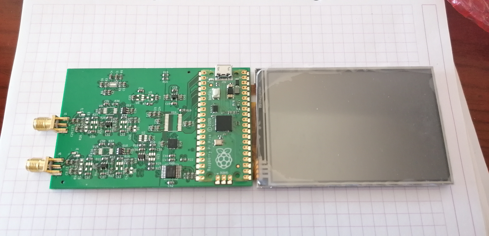
Final result
GUI
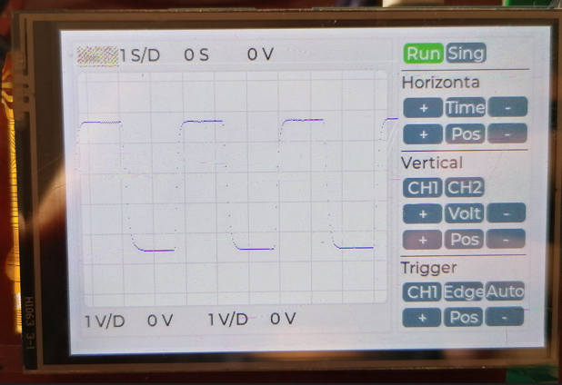
Diagram overview
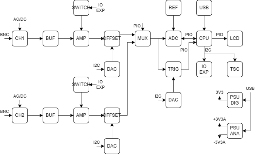
In this diagram we see all the elements of the oscilloscope.
- The power supply comes from the USB and is regulated independently for the analog and digital parts.
- Each analog stage is made up of 3 op amps, a gain selector and a DAC for the offset. The selection between AC/DC is done manually by means of a jumper. (Normally this is done with a relay)
- The acquisition block is composed of the multiplexer, the ADC and the trigger. All controlled by PIO.
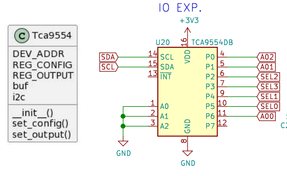
- An I2C bus controls 3 DACs, a TSC and an IO expander (which controls the analog stage).
- The LCD is also PIO controlled.
Scheamtic
In the general scheme we see the power part at the top left, the two input channels at the bottom left and the digital part at the top right.

Power Supply
The power supply takes the 5V from the USB and provides 3 voltages:
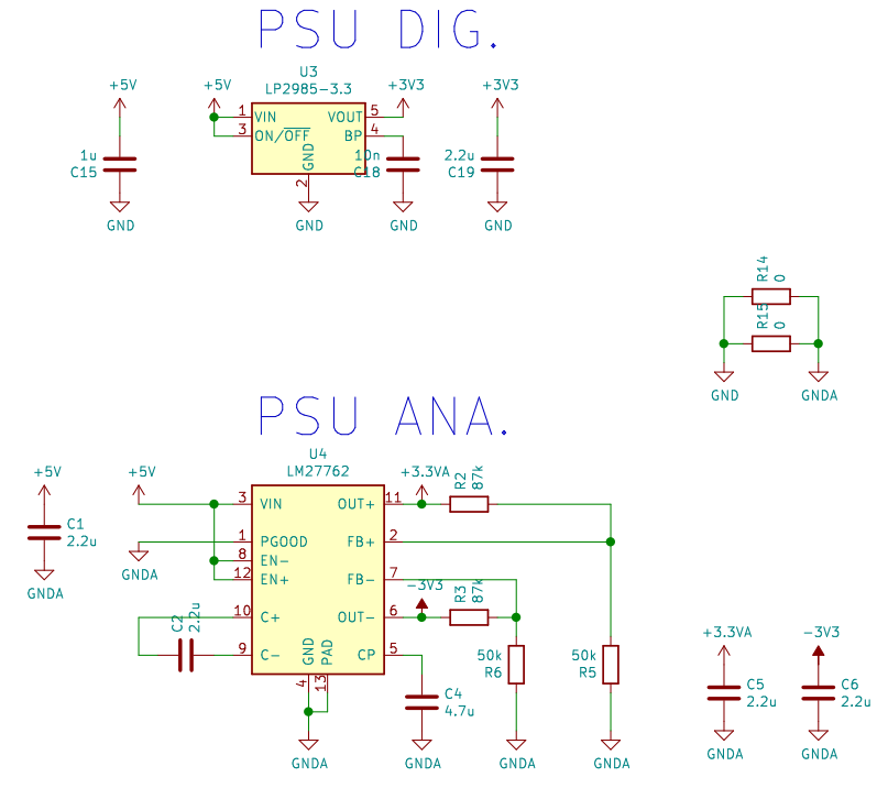
- 3V3 that will be used for all digital electronics.
- Symmetric 3V3A that will be used for all analog electronics
The integrated LM27762 is a symmetrical regulated source that is capable of generating the negative part using only one capacitor (C2).
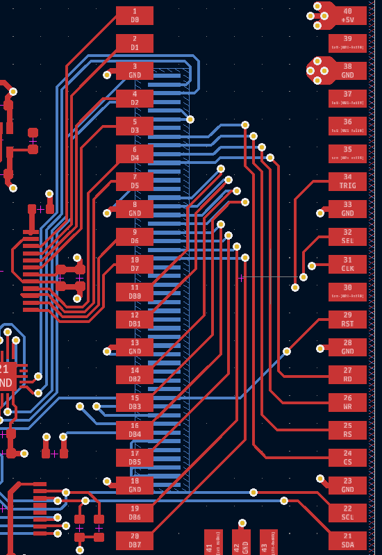
CPU block
The main block consists of the ADC, the CPU, and the LCD.

All CPU pins are occupied:
- 8 pins for the ADC bus.
- 3 pins for MUX, ADC and TRIG control.
- 8 pins for the LCD bus.
- 5 pins for LCD control.
- 2 pins for an I2C bus.
- 1 pin for LCD and TSC reset.
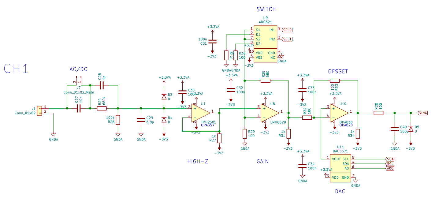
Analog front end
The analog input stage is made up of several passives, 3 opamps, a multiplexer and a DAC.
The input impedance is marked by resistors R24+R26, which is 780 KOhm.
The AC filter (set by C27) has a cutoff frequency of 20 Hz.
The gain of this stage is (100/(680+100)) = 0.12. As the supply of the amplifiers is ±3.3V, this gives us a maximum input voltage of ±27V.
Front end simulation
The simulation has been carried out with the Texas Instruments software and all the components have a SPICE model. The bandwidth is greater than 100 MHz and the gain remains constant throughout the entire spectrum.

Analog miscellaneous
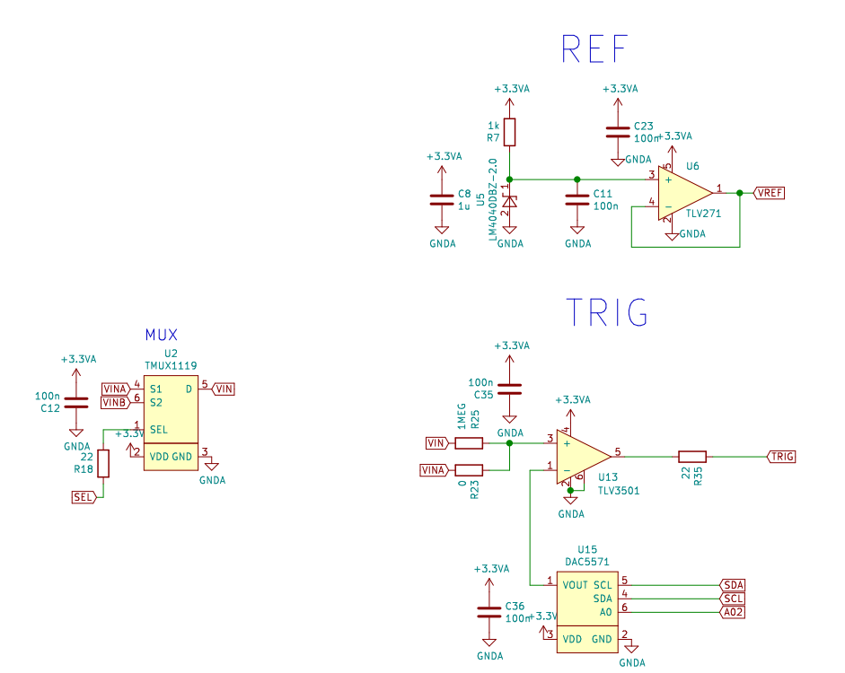
The reference is implemented with a 2.048V zener connected to an opamp configured as an emitter follower.
The trigger is implemented with an 8-bit DAC and a comparator. The TLV3501 is a high speed comparator, with a delay time of 4nS.
The multiplexer is controlled from the CPU and allows switching from one channel to another. Initially the intention was to do it at 50MHz, but later I verified that these components have a limitation that prevents them from working in this way.
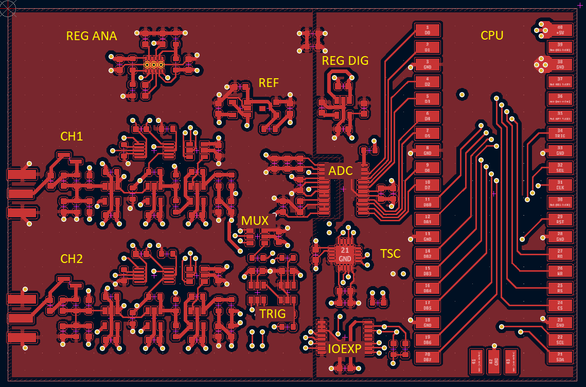
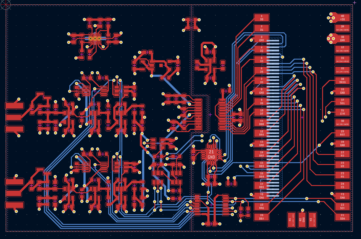
PCB component placing
The components are grouped in clusters with the same functionality and then these clusters are arranged from left to right, starting with analog clusters and ending with digital ones. Also, the power supplies and analog miscellaneous are placed on the upper area of the top layer.
Each cluster is routed on the top layer, connected to the power layers with vias and to other clusters through the bottom layers.

Cluster routing
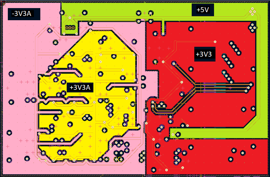
The analog power supply routing should be as clean as possible. All nets should be as short as possible, specially feedback nets and as wide as possible, specially power nets.
The power input comes from 5V from the upper part and then ±3V3 goes out to the lower part.
Analog PSU routing
The ADC is located between the analog and digital planes. It has the analog part on the left and the digital part on the right.

The analog part is made up of the power pins, the ADC input itself, and the reference. The digital part is made up of the data and control pins.
In the analog part, the routing of the power pins has priority over the signal pins and the latter arrive through the bottom layer.
ADC routing
The front end is the cluster with the most components and is made up of 5 devices. The signal goes from left to right and the power is distributed like a tree, even if the complete copper plane makes this detail hidden. The control lines for the analog switch and i2c lines for the dac came through the bottom layer.

Front end routing
As all clusters are routed on the top layer and power pins are easily connected to power panes, the inter-cluster routing should be an easy task. Here are the results.

Inter-cluster routing
As all clusters are routed on the top layer and power pins are easily connected to power panes, the inter-cluster routing should be an easy task.
Power planes
The power planes need to be carefully drawn, and the results are influenced by the cluster placement from the first chapter. The main rule is: connect all vias with the bigger copper area you can draw.
Ground planes
For the ground planes, the same rule is applied, but normally these are easier.

LCD bus routing
The LCD is connected using an 8-bit 8080 interface and pretends to achieve rates of 20MHz. These signals are routed as short as possible using top and bottom layers.
Software
The software is based on three layers:
- HAL, that is composed of one python class for each device of the board.
- GUI, that is composed by some LVGL drivers and some high level layer that offers a similar “dear pygui” API.
- Scope, that is composed by the state of the object and allows the acquisition procedure.
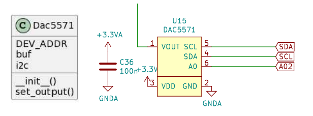
One of the simplest elements of the HAL is the DAC. It only uses an I2C port and one GPIO. To set the output value, this class only needs to perform a single write to a specific address in the I2C. There are 3 DACs on the board, all connected to the same I2C. The DAC uses a digital input pin to set its own address, and this is used as an enable pin needed to select only one DAC. As the RP2040 has not enough pins, the A0 pin is connected to the IO_EXP and the software handles it to access the desired DAC.
DAC class
The input-output expander is controlled via I2C bus and handles the 3 DAC A0 pins mentioned above and the analog switches.
The class offers methods to configure each pin (but in this project all should be output) and also to set the value.
IO expander class
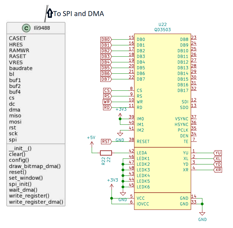
The TFT is the second most complex device of the board, only after the CPU. The LCD supports different interfaces, but this hardware sets it to 8-bit 8080 interface via M0:2 pins.
This interface has 8 bits of data and 4 control signals. The LCD initialization requires setting the value of about 20 registers to prepare the LCD for work. When this is done, only 2 operations are needed: 1 set the window and 2, send the data. This is the optimal way to work with LCDs. The software draws in the image in a buffer, then the buffer is transferred to the LCD. As the LCD has its defined working region, the full data transfer can be done easily and fast using the DMA.
The current version only supports a previous prototype version that used SPI, and is expected to build an Intel 8bit 8080 interface using PIO in the future.
TFT class
ADC class
The ADC08100 uses 8 signals for data and one signal for clock, all handled via PIO. The user sets the buffer address, the size and the sample rate and sample count and then the PIO+DMA does the capture. The number of samples captured is used to configure the DMA and the sample rate is directly derived from the CPU clock, note that the number of samples can be bigger than the buffer size and the DMA will store the data in a circular buffer way.
The PIO program has only two instructions. 1 Read the input pins and 2, push them to the DMA. Thanks to the PIO side”sideset” instructions, at the same time than previous instructions, the ADC clock is generated, so it can read at the same moment that the ADC outputs are available.

Some points to comment about the DMA circular buffer alignment and micropython buffer alignment. The DMA periferials can only perform circular modes in 2s complements aligned buffers, it means that if your buffer has 256 bytes, it should be placed in address 0xXXXXXX00 to 0xXXXXXXFF. As micropython does not allow alloc a buffer in the specific address, the only way to bypass this limitation is to alloc a bigger buffer that surely has a 00-FF range and then use it.

The multiplexer should be managed during conversion in the case that two channels are needed. This management can be done via the ADC PIO program. By the time I was able to do the hardware tests, I discovered that this multiplexer is not fit for purpose in this design. The multiplexer has a settling time, which occurs when changing channels, which prevents switching to 50MHz, so the ADC would not be able to work at maximum frequency if both channels were used. This is a limitation of the current prototype and a point to improve in the future.
Channel multiplexer
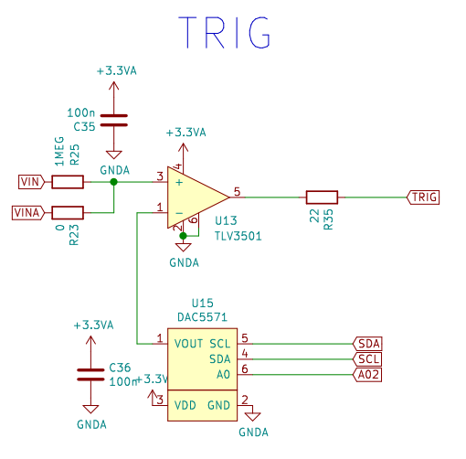
The trigger is based on a DAC and a comparator. I personally never realize the difference between an op amp and a comparator. The difference is related to the speed, when the ADC is saturated and needs to return to a linear state, it has a limitation parameter called Overload Recovery Time, in order of 100nS. The comparators never operate in the saturation region, so they don’t have this effect at all. There is also a propagation delay that must accomplish some requirements, but the TLV3501 easily detects signals at 200MHz.
The DAC module is used to generate the threshold value. Note that this DAC is powered from the digital domain and maybe this is something that can be changed in future versions.

Trigger
The trigger PIO program uses a special trick for its operation. The user can program PRE and POST sample count and then the ADC PIO is stopped. The pre-trigger samples retain the data before the trigger event. This is done because the ADC data is stored in a continuous circular buffer. After the trigger is detected, a counter is decremented to store de post-trigger samples and then a simple value is pushed out to the DMA. The trick is that this DMA is configured to write its value to the control registers of the DMA used by the ADC, stopping it. This simple trick allows the whole machinery ADC+TRIGGER without any CPU intervention.

Touch screen controller
The TSC is a simple I2C device that can handle the resistive touch screen. It has some registers to read the raw ADC values of the X and Y coordinates. The class also averages these values and converts them to pixel coordinates via calibration values.


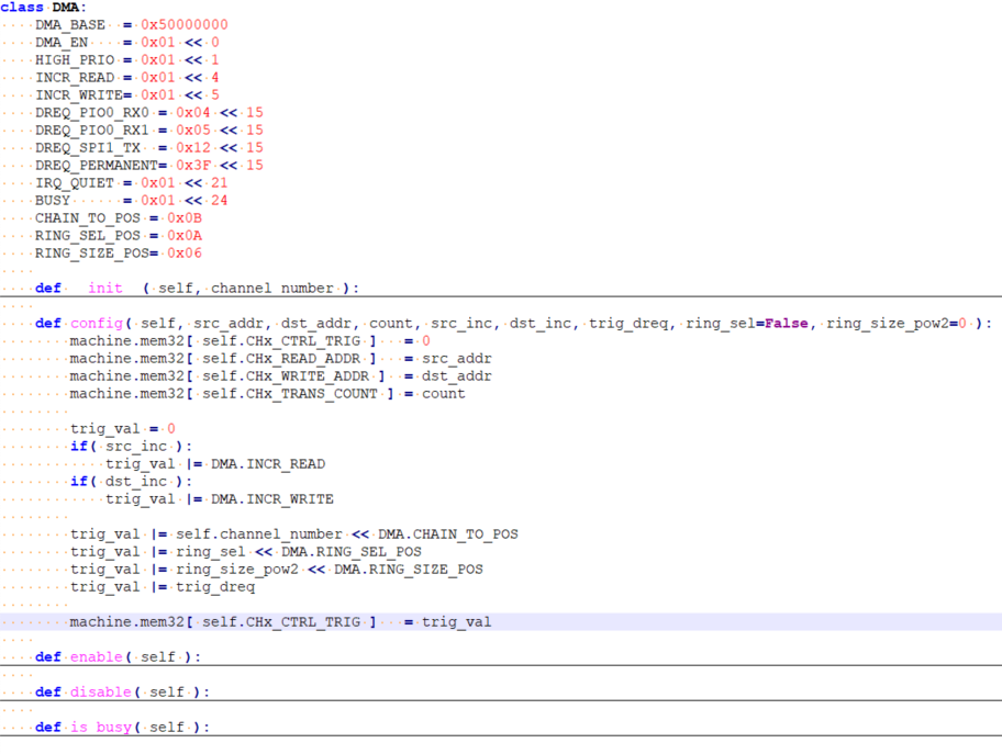
DMA
The DMA class is used from the ADC, trigger and LCD classes. Is responsible for DMA configuration and usage and is a simplified interface for the DMA control registers.
The usage is really easy: configure, enable, wait and disable. This simple procedure allows transfer of memory-to-memory or peripheral-from/to-memory at max clock speed.
The scope class implements all the scope internals, and its representation in the screen also handles the whole acquisition procedure (all isolated in one function).
The initial action is to define the user interface. This is done by creating a tree organized with rows and columns where some elements like buttons and labels are added. This GUI build method is derived from dearpygui and was added to LVGL as an extra feature to simplify the application design.
The GUI is defined in the build_ui method of the class and the behavior is defined via the callbacks added to the GUI. Most of them simply store the user values (note that there is almost a callback for each button on the screen). Then the cb_run callback configures the ADC and performs the acquisition.


Display driver
The display driver is the glue between LVGL and our LCD. It initializes the LVGL library, sets its drawing buffers and defines the display flush callback and the touch screen read callback.
LVGL uses the drawing buffer to draw a specific part of the GUI. When the drawing is done, it calls its display flush callback to draw(send) this buffer to the LCD. The callback parameters are the drawing coordinates and the buffer address, exactly the parameters that we need to draw the LCD using DMA. If the double buffer is used, we can interchange the buffers so DMA and CPU exchange the buffers each time.
The input read callback is called periodically by LVGL. It should read the touch screen and simply return the state (pressed/not pressed) and the X/Y coordinates to the LVGL library.

DearPyGUI
DearPygui is a python library that allows defining the GUI by using context managers and this feature simplifies the GUI design. That is why I created a simple module to offer this functionality to LVGL. This module defines a Row and Column classes that support context management to build a layout aligned widget trees.
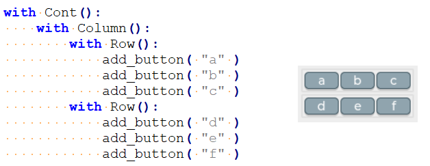
DearPyGUI emulation over LVGL

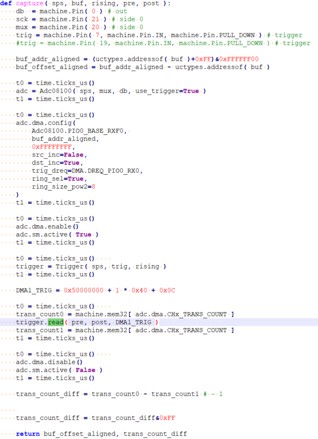
Capture block
The capture is performed when the user presses the “run” button. It is performed using the ADC and trigger objects commented in previous chapters. After the configuration is performed, the ADC is started and then the trigger. Then will state on trigger read funcion, that is waiting for DMA to finish, that is waiting inside a PIO loop to detect the rise/fall event. When this happens, the acquisition waits a little bit more to fill the buffers and then stops and the data is then used to update an LVGL widget chart.